Introduction
Argon fluoride (ArF) immersion lithography is the dominant patterning technology behind the chips powering smartphones and data center processors. Despite the emergence of extreme ultraviolet (EUV) lithography for the most critical layers, ArF immersion handles the majority of patterning steps at advanced nodes—including sub-10nm production—due to its proven reliability, throughput, and cost-effectiveness.
At TSMC's 5nm and 3nm nodes, ArF immersion systems pattern 30 to 55 layers per chip, while EUV handles just 14 to 25 critical layers.
The mechanism behind it, though, is rarely explained in full. How does an argon-fluoride gas mixture, a photon beam, a thin layer of ultrapure water, and a silicon wafer interact to print circuit features measured in nanometers? This guide walks through each stage of the process—from gas excitation through pattern development—with enough technical detail to make the physics clear.
TL;DR
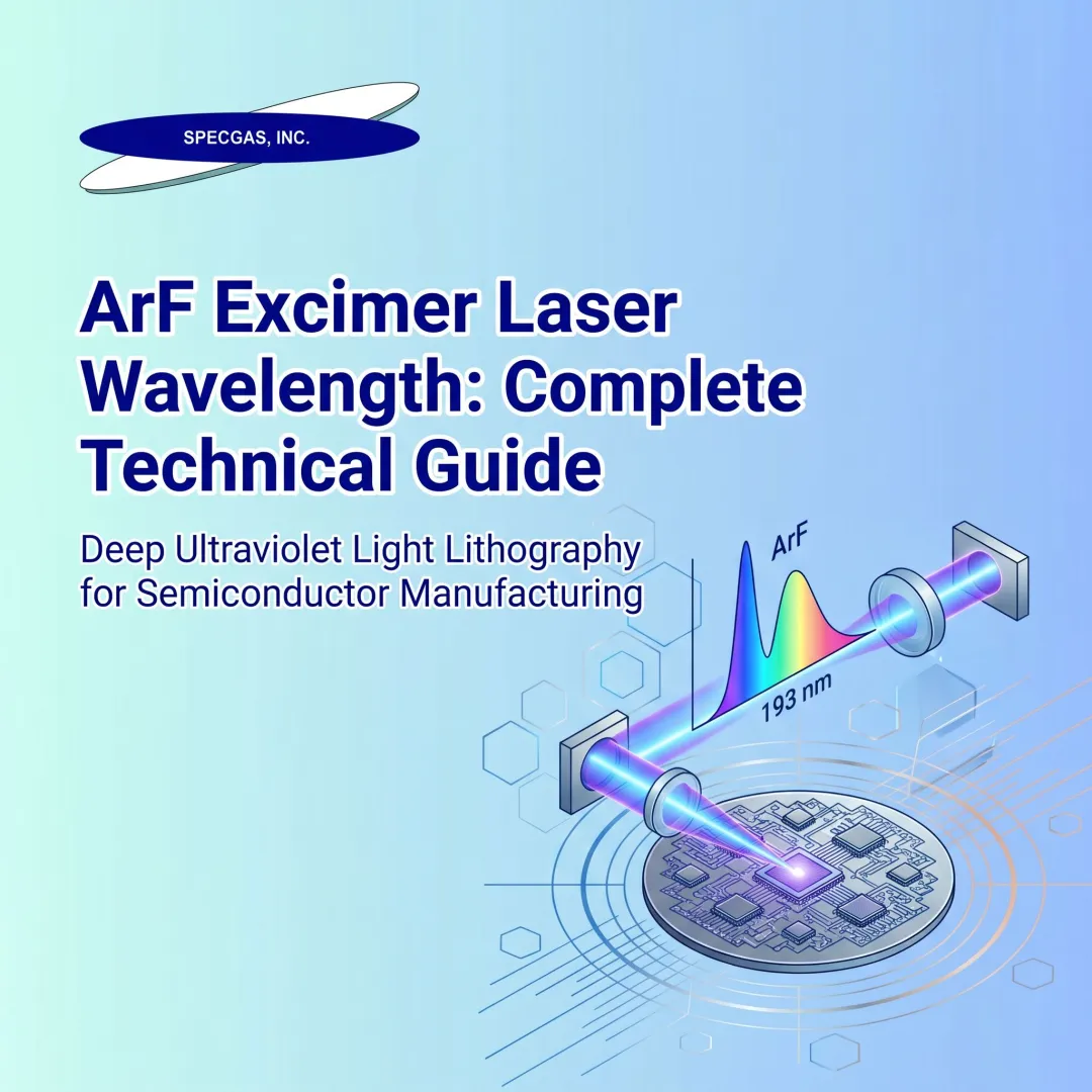
- ArF immersion lithography uses a 193nm laser generated by an argon-fluoride gas mixture to expose nanoscale patterns onto photoresist-coated silicon wafers
- Ultrapure water between the lens and wafer pushes numerical aperture beyond 1.0, surpassing dry-system resolution limits
- Water reduces effective wavelength from 193nm to ~134nm by increasing refractive index to 1.44
- Exposure follows five tightly controlled steps: laser generation, beam conditioning, mask projection, immersion exposure, and chemical development
- Single-exposure resolution reaches 38-40nm; multi-patterning extends capability to sub-10nm nodes
What Is ArF Immersion Lithography?
ArF immersion lithography is a form of deep ultraviolet (DUV) photolithography that uses a 193-nanometer laser produced by an argon fluoride excimer laser, combined with an ultrapure water layer between the projection lens and the wafer, to print nanoscale circuit patterns onto semiconductor substrates.
The technology emerged in the early 2000s to solve a critical roadblock. Attempts to shrink chip features using 157nm fluorine lasers ran into serious material physics problems with calcium fluoride optics — intrinsic birefringence, a lack of transparent pellicle materials, and high resist absorption. Water immersion at 193nm provided a 45% resolution gain over dry 193nm, compared to only 23% from transitioning to dry 157nm, making it the clearly superior path forward.
ArF immersion lithography is distinct from dry ArF lithography, which operates in air with a maximum numerical aperture (NA) below 1.0 due to total internal reflection limits. It differs fundamentally from EUV lithography, which uses 13.5nm light in near-vacuum conditions. The immersion element — not the ArF laser alone — is what enables sub-65nm patterning at this wavelength.
Even as EUV handles the most critical layers at leading-edge fabs, ArF immersion systems continue to pattern the majority of layers on advanced chips. According to ASML, DUV lithography systems remain "the workhorses of the industry, producing the majority of layers in microchips." At TSMC's leading nodes, ArF immersion's role remains substantial:
- N5 (5nm) node: ~50-55 of roughly 85 total layers patterned using DUV
- N3 (3nm) node: 30-40 layers remain on DUV, even with 25-28 EUV layers in use
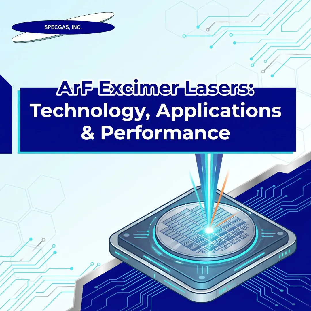
How Does ArF Immersion Lithography Work?
ArF immersion lithography operates through a tightly sequenced series of stages, each dependent on the one before. Understanding each stage clarifies why the system achieves resolutions that would otherwise be physically impossible with 193nm light in air.
Laser Initiation and Gas Excitation
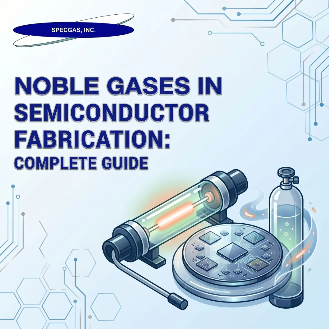
The process begins inside the ArF excimer laser cavity, where 193nm photons are generated through a precisely controlled discharge mechanism. A high-voltage electrical pulse (fired at multi-kilohertz frequencies) energizes a pressurized mixture of neon, argon, fluorine, and xenon (typically at 3.4 atmospheres). The discharge creates a short-lived excited complex (ArF*), which emits coherent ultraviolet light at 193nm as it decays and dissociates into argon and fluorine atoms.
Modern production ArF light sources operate at pulse repetition rates between 4,000 Hz and 7,800 Hz to support high scanner throughput. For example, Cymer's XLR 1000ix operates at 6,750 Hz, while Gigaphoton has demonstrated systems at 7,800 Hz.
Gas mixture quality is critical to process stability. The argon-to-fluorine ratio, purity, and buffer gas composition directly affect laser output power, pulse energy consistency, and beam coherence—all of which translate into critical dimension (CD) uniformity on the wafer. Small amounts of gaseous impurities (above 10 ppm of oxygen, CF₄, or HF) strongly deteriorate laser output energy and stability. Conversely, trace xenon additions (around 10 ppm) enhance preionization density, improving discharge homogeneity and pulse-to-pulse energy stability.

Suppliers like SpecGas provide NIST-traceable ArF excimer laser gas blends with proprietary cylinder treatment processes designed to maintain reactive gas mixture stability over time, ensuring that laser performance remains consistent across extended production runs.
Core Operation: The Immersion Exposure Mechanism
After exiting the laser cavity, the 193nm beam passes through an illumination system that conditions it for uniform illumination and coherence control before reaching the reticle. The reticle (photomask) carries the circuit pattern in chrome or phase-shifting material at 4× the target size.
From there, a catadioptric projection lens (combining refractive and reflective elements) demagnifies the pattern by 4× and focuses it onto the wafer surface.
The Immersion Effect
The key departure from dry lithography is at the final lens element: instead of facing air (refractive index n = 1.0), it faces a continuously circulating layer of ultrapure deionized water with a refractive index of approximately 1.44 at 193nm. Because numerical aperture is defined as NA = n × sinθ (where θ is the half-angle of the maximum light cone), replacing air with water allows NA values above 1.0. ASML's NXT production systems achieve 1.35 NA, which directly improves resolution according to the Rayleigh equation:
Resolution = k₁ × λ / NA
where k₁ is a process-dependent factor, λ is wavelength, and NA is numerical aperture.
Water immersion reduces the effective wavelength of light from 193nm to approximately 134nm (193nm ÷ 1.44), enabling finer feature resolution. Additionally, immersion improves depth of focus (DOF) compared to dry systems at the same NA. Research has demonstrated approximately 1.8× DOF improvement with immersion versus dry exposure at equivalent NA and illumination conditions, because water reduces the refractive angle of exposure beams entering the resist.
Water Management System
The immersion system supplies ultrapure water continuously through an immersion hood surrounding the final lens. The water undergoes rigorous treatment:
- Degassing to suppress dissolved oxygen below 70 ppb (or 10 ppb), preventing micro-bubble formation
- Particle filtration to remove contaminants larger than 30nm
- Total organic carbon (TOC) reduction below 50 parts-per-trillion through UV treatment
- Temperature control to ±0.01°C, because the refractive index temperature coefficient (dn/dT) is approximately 10⁻⁴/°C — a 0.01°C shift causes roughly 1nm defocus

Any bubble, particle, or temperature variation in the water layer creates a localized defect in the exposed pattern, making water quality control essential to yield.
Regulation and Control
Maintaining imaging quality across varying conditions requires multiple real-time control systems. The scanner uses interferometric or encoder-based stage positioning (in advanced NXT-class systems) to hold overlay accuracy at sub-nanometer levels between successive exposures. The wafer stage moves at speeds up to 500mm/s while the water meniscus must remain confined under the lens without leaving droplets behind — a challenging fluid dynamics problem.
Resist-Water Interface Control
The photoresist coated on the wafer must maintain a sufficiently high dynamic receding contact angle (typically above 70°) to prevent the water meniscus from leaving droplets on the wafer surface as the stage moves. Watermark defects from residual droplets degrade local resist photosensitivity and cause pattern defects.
Topcoats or specially engineered immersion resists with hydrophobic surfaces manage this interface, enabling high-speed scanning without water leakage.
Post-Exposure Bake (PEB)
After exposure, the chemically amplified resist undergoes a post-exposure bake at a precisely controlled temperature (typically 90–130°C depending on resist formulation). PEB activates the photoacid-catalyzed deprotection reaction, converting exposed areas from developer-insoluble to developer-soluble. Temperature uniformity across the hotplate must be maintained within ±0.1°C because PEB temperature directly controls critical dimension through acid diffusion length — variations of 1–5nm per degree Celsius are typical.
Output: Pattern Development and Transfer
After PEB, the wafer is developed in aqueous tetramethylammonium hydroxide (TMAH) solution at 2.38 wt% concentration. The developer dissolves the deprotected (exposed) resist, leaving behind a patterned resist layer that replicates the mask pattern at 1/4 scale.
Resolution Capabilities:
- Single exposure (1.35 NA): 38–40nm half-pitch
- Self-Aligned Double Patterning (SADP): ≤20nm half-pitch
- Self-Aligned Quadruple Patterning (SAQP): 10–19nm half-pitch
- Self-Aligned Octuple Patterning (SAOP): Sub-10nm half-pitch (demonstrations at 6–9nm)

The developed resist pattern serves as a stencil mask for etching, ion implantation, or thin-film deposition steps that transfer the circuit pattern into the silicon or dielectric layers below. The quality of the resist pattern — its CD uniformity, line-edge roughness, and sidewall profile — directly controls the electrical performance and yield of the finished transistors.
Where ArF Immersion Lithography Is Used
ArF immersion lithography is applied repeatedly throughout semiconductor fabrication—often at 40 or more lithographic layers per chip—to pattern gate structures, contact holes, metal interconnects, and other critical features. The most performance-sensitive layers (gate, contact, and metal-1) typically use immersion with aggressive off-axis illumination and multi-patterning to reach the smallest features.
These steps run inside ISO Class 1 cleanrooms, in fully automated litho-clusters where the track (coating and development system) is directly interfaced with the immersion scanner to minimize delay between exposure and post-exposure bake (PEB). All of this is optimized for high-volume manufacturing at 300mm wafer sizes.
ArF immersion spans nearly every advanced chip category:
- Logic chipmakers — CPU, GPU, and mobile SoC production
- DRAM manufacturers — DUV immersion still dominates at 1a/1b/1c nodes, with only 1–6 EUV layers added
- NAND flash producers — 3D vertical scaling reduces the need for EUV-level pitch resolution
Even at 3nm logic fabs, where EUV handles the most critical layers, ArF immersion still accounts for the majority of patterning steps by count. That ratio is unlikely to shift dramatically until high-NA EUV tools scale beyond their current limited deployment.
Conclusion
ArF immersion lithography achieves sub-wavelength resolution by combining a 193nm excimer laser, a precisely controlled ultrapure water immersion layer, high-NA optics, and chemically amplified resists into a precisely sequenced process that translates mask patterns into transistor-scale features on silicon. Each stage depends on the precision of every component in the chain—from the gas blend that generates the laser to the water purity that enables the immersion effect.
For semiconductor process engineers, equipment managers, and gas procurement professionals, understanding how each system element affects imaging outcomes directly informs sourcing and process decisions. Excimer laser gas mixture quality sits at the center of that chain. Key variables include:
- Argon-to-fluorine ratios: Precise blend composition determines laser output power and spectral stability
- Purity control: Contaminant levels at the PPB scale affect beam coherence and CD uniformity on the wafer
- Cylinder treatment: Reactive gas stability over the cylinder's service life prevents output drift between refills
SpecGas Inc. produces NIST-traceable ArF excimer laser blends using a proprietary internal cylinder treatment process developed specifically for reactive gas stability—supplying the consistency that high-volume advanced node production requires.
Frequently Asked Questions
What is the difference between DUV and immersion lithography?
DUV (deep ultraviolet) lithography refers to the wavelength class—193nm or 248nm—while immersion lithography refers to the technique of placing a high-refractive-index fluid (typically water) between the final lens and the wafer. Immersion is a modification applied to DUV systems to increase effective NA and resolution beyond what dry DUV can achieve.
What is the difference between EUV and DUV?
EUV (extreme ultraviolet) uses 13.5nm light—roughly 14× shorter wavelength than ArF DUV at 193nm—enabling single-exposure patterning of sub-30nm features. DUV immersion operates at 193nm but achieves comparable results at certain nodes through multi-patterning, at lower tool cost but with more process steps.
Why is water used as the immersion fluid in ArF immersion lithography?
Water is well-suited for ArF immersion because its refractive index (≈1.44 at 193nm) is higher than air, directly increasing the system's effective NA. It is also highly transparent to 193nm light (absorption coefficient ≈0.036 cm⁻¹), chemically stable under UV exposure, and already integrated into fab infrastructure—making it practical for high-volume manufacturing.
What is the maximum numerical aperture achievable with ArF immersion lithography?
Water-based immersion is fundamentally limited by water's refractive index of 1.44, placing the practical NA ceiling around 1.35. Production systems from ASML (e.g., the NXT:2100i and NXT:2050i) operate at up to 1.35 NA, which represents the limit of what is achievable with water as the immersion medium.
What semiconductor node sizes can ArF immersion lithography reach?
Single-exposure ArF immersion can reliably print features at the 38-40nm half-pitch range. With double and quadruple patterning techniques, the same systems have been used to pattern features at sub-10nm nodes, where multiple interlaced exposures together achieve the final pattern pitch.
What gases are used in the ArF excimer laser, and why does gas quality matter?
The laser cavity is filled with a precise mixture of argon and fluorine diluted in buffer gases such as neon or helium. The mixture ratio, purity, and reactive gas stability directly affect laser output power, pulse energy consistency, and beam coherence—all of which translate into CD uniformity and defect rates on the wafer.