Introduction
Modern semiconductor chips, from smartphones to AI processors, cannot be manufactured without a small group of chemically inert elements: the noble gases. Reactive gases do the cutting and depositing, but noble gases provide the stable, contamination-free environments and precision energy that make each step possible. At sub-5nm geometries, where billions of transistors occupy a chip the size of a fingernail, even trace contamination from an off-spec gas can render an entire wafer lot defective.
This guide covers which noble gases are used across semiconductor fabrication, why their unique chemistry makes them indispensable, and how purity specifications translate directly to device yield.
Whether you're a process engineer qualifying suppliers or a procurement manager navigating supply risks, understanding argon, helium, neon, krypton, and xenon is critical to protecting fab uptime and product quality.
Key Takeaways
- Each noble gas fills a non-interchangeable role: sputtering, CVD, lithography, and ion implantation
- Full outer electron shells make noble gases chemically inert, preventing unwanted reactions in plasma and high-temperature processes
- 6N purity (99.9999%) is the floor—trace oxygen or moisture causes direct yield loss
- Neon, krypton, and xenon supply chains are geographically concentrated and vulnerable to disruption
- NIST-traceable blending ensures process repeatability across calibration and production gas applications
Why Noble Gases Are Uniquely Suited for Semiconductor Manufacturing
Complete Electron Shells Deliver True Inertness
Noble gases occupy Group 18 of the periodic table and possess fully occupied outer electron subshells. This closed-shell configuration results in near-zero chemical reactivity — they don't form true chemical compounds under standard conditions. In semiconductor environments where wafers undergo extreme temperatures (up to 1000°C) and high-energy plasma bombardment, this complete lack of reactivity is non-negotiable.
Nitrogen Isn't Truly Inert
While nitrogen is cheaper and often called "inert," it can react at the temperatures and energies common in semiconductor equipment. During high-temperature CVD or within plasma chambers, nitrogen forms unwanted nitrides with silicon and metal films, compromising purity. Noble gases remain chemically passive, ensuring they never interfere with deposition chemistry or etch selectivity.
Argon's Dual Advantage: Inertness Plus Plasma Performance
Where nitrogen fails, argon delivers on both counts. Argon ionizes readily under RF power (ionization energy: 15.759 eV), forming stable, controllable plasmas critical to both deposition and etching. Free electrons collide with argon's outer shell, creating positively charged Ar⁺ ions that bombard target materials with precise momentum transfer.
This dual capability makes argon indispensable across fab process steps:
- Chemical inertness: Never reacts with silicon, metal films, or process chemistry at any fab-relevant temperature
- Plasma stability: Produces consistent, controllable ion bombardment under RF conditions
- Momentum transfer: Ar⁺ ions deliver predictable energy to target surfaces for uniform deposition and etch rates
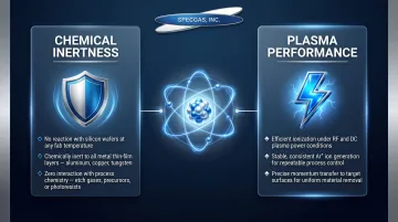
That last point matters for gas purity: even trace contaminants in argon supply can introduce reactive species into otherwise inert plasma environments, which is why semiconductor-grade argon specifications are so demanding.
Noble Gases Across Major Semiconductor Fabrication Processes
Sputtering and Physical Vapor Deposition (PVD)
Argon: The Primary Sputter Medium
In magnetron sputtering, argon plasma is ionized under RF or DC power. The resulting Ar⁺ ions bombard a target material (titanium, tungsten, copper), physically ejecting atoms that deposit as a thin film on the wafer. Key process parameters:
- Atomic mass: 39.948 u — sufficient momentum transfer without altering film chemistry
- Operating pressure: 0.2 to 4 Pa typical
- Purity requirement: 99.999% (5N) minimum for advanced node deposition
Helium: Precision Wafer Cooling
Helium's thermal conductivity (155.7 mW·m⁻¹·K⁻¹ at 300 K) is nearly nine times higher than argon's (17.7 mW·m⁻¹·K⁻¹). In PVD systems, helium flows between the wafer and electrostatic chuck (ESC), efficiently conducting heat away and maintaining precise substrate temperature. This prevents thermal stress in deposited films and ensures process uniformity across the wafer.
Chemical Vapor Deposition (CVD) and Plasma-Enhanced CVD (PECVD)
Carrier and Diluent Roles
Where PVD relies on noble gases as the plasma medium, CVD processes depend on them as inert carriers. Argon and helium transport volatile precursor gases (silane, TEOS) to the wafer surface at controlled concentrations without participating in deposition chemistry. Diluting reactive precursors with noble gases stabilizes the process and enables fine control over deposition rate and film uniformity.
Plasma Activation at Lower Temperatures
In PECVD, argon sustains the plasma that activates precursor decomposition at lower temperatures than thermal CVD. This enables film deposition on temperature-sensitive device structures—critical for back-end-of-line (BEOL) processing where aluminum interconnects would melt under traditional CVD temperatures.
Dry Etching and Plasma Etching
Argon: Diluent and Physical Etch Component
Etching introduces a different demand profile from deposition. In reactive ion etching (RIE) and inductively coupled plasma (ICP) systems, argon is mixed with reactive gases like CF₄, Cl₂, or SF₆. It stabilizes plasma density while contributing physical sputtering — the combination that produces anisotropic (directional) etch profiles essential for high-aspect-ratio features at advanced nodes.
Helium Backside Cooling
During plasma etching, helium flows between the wafer and ESC to conduct heat away. Watch for these warning signs of inadequate cooling:
- Leak-by flows exceeding 20 sccm indicate poor wafer-chuck contact
- Non-uniform helium pressure causes localized etch rate variation
- Insufficient clamping force reduces heat transfer and increases defect risk
Photolithography and Excimer Lasers
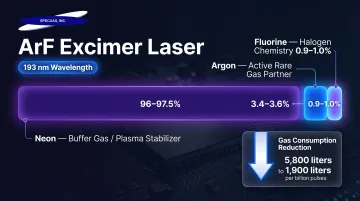
Neon: The Backbone of ArF Lithography
Photolithography places the most stringent purity demands of any noble gas application in fab. ArF excimer lasers (193 nm wavelength) — the workhorses of deep-UV patterning at advanced nodes (≤38 nm) — operate on a tightly controlled gas mixture:
| Gas | Role | Approximate Concentration |
|---|---|---|
| Neon | Buffer gas / plasma stabilizer | 96–97.5% |
| Argon | Active rare gas partner | 3.4–3.6% |
| Fluorine | Halogen chemistry | 0.9–1.0% |
Without consistent, high-purity neon supply, the plasma discharge destabilizes and wavelength precision degrades — making precise sub-10 nm feature patterning impossible.
Krypton for Legacy Nodes
KrF excimer lasers (248 nm wavelength) use krypton as the active rare gas, with neon as the majority buffer gas and fluorine for halogen chemistry. These lasers serve legacy nodes (80–250 nm) for metal, via, and implant layers. Though older technology, KrF systems remain in production and drive continuous krypton demand.
Continuous Consumption Through Gas Refresh
Excimer laser gas mixtures are regularly refreshed during operation. While manufacturers like ASML/Cymer have reduced ArF laser gas consumption from 5,800 liters per billion pulses to 1,900 liters per billion pulses through recycling optimization, consumption remains substantial—especially as lithography passes per wafer increase at advanced nodes.
The Rarer Noble Gases: Neon, Krypton, and Xenon in Advanced Applications
Neon: Critical to Advanced-Node Lithography
Neon's role in 193 nm ArF lithography makes it the highest-volume rare noble gas consumed in advanced fabs. As chip geometries shrink, lithography passes per wafer increase, driving neon demand steadily higher.
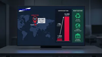
Prior to 2022, Ukraine dominated global supply — providing approximately 45–54% of the world's semiconductor-grade neon and up to 90% of highly purified neon imported by the United States. That concentration was a legacy of Soviet-era steel mills equipped with large Air Separation Units (ASUs) capable of rare gas extraction.
In February 2022, the Russian invasion halted Ukrainian neon production. The supply shock was immediate:
- Wholesale neon prices in China spiked to 16,000 yuan (~$2,500) per cubic meter in March 2022 — nearly nine times the pre-invasion price of 1,850 yuan
- Global neon consumption for chip production had reached 540 metric tons in 2021, amplifying the shortage's scale
- Fabs responded by deploying on-site recycling systems and aggressively qualifying new suppliers outside Eastern Europe
Krypton: High-Performance Etching and Legacy Lithography
Krypton's higher atomic mass (83.798 u versus argon's 39.948 u) delivers more efficient momentum transfer when sputtering heavy elements. This makes krypton valuable in specialized etch applications where argon's lighter mass is insufficient. Krypton is also the active gas in KrF excimer lasers for 248 nm photolithography at legacy nodes, sustaining ongoing demand despite the industry's shift toward smaller geometries.
Xenon: Ion Implantation, Annealing, and EUV
Ion Implantation and Flash Annealing
Xenon's large atomic mass makes it ideal for ion implantation — it delivers precisely controlled momentum to dopant ions without introducing unwanted chemical doping effects.
Arc flash lamps using xenon are a separate but equally critical application: they enable millisecond-scale thermal annealing for ultra-shallow junction (USJ) formation. These lamps emit intense, short-wavelength light that selectively heats the wafer surface to activate dopants like boron without causing unwanted bulk diffusion.
Emerging EUV and Hard Mask Applications
Beyond implantation, xenon is finding new roles in extreme ultraviolet (EUV) plasma light sources and as a sputter etch species for hard mask patterning. As advanced nodes adopt EUV lithography, xenon demand will grow.
That growth puts real pressure on sourcing. Xenon's atmospheric abundance sits at just 0.086 parts per million by volume — making it one of the rarest stable gases on Earth — so fabs sourcing xenon for EUV face the same supply concentration risks that blindsided the industry with neon in 2022.
Semiconductor-Grade Purity: What UHP Standards Mean in Practice
Ultra-High Purity Specifications
Semiconductor-grade noble gases typically meet 6N (99.9999%) purity or higher, with specific impurity limits in the parts-per-billion (ppb) range:
| Gas | Grade | Purity | O₂ Limit | H₂O Limit | THC Limit | N₂ Limit |
|---|---|---|---|---|---|---|
| Neon | 5.0 | ≥99.9990% | <0.5 ppmv | <1.0 ppmv | <1.0 ppmv | <2.0 ppmv |
| Argon | 6.0 | ≥99.9999% | ≤0.5 ppmv | ≤0.5 ppmv | ≤0.1 ppmv | ≤0.5 ppmv |
Even sub-ppb levels of oxygen or water vapor can oxidize sensitive metal films or introduce defects in gate dielectrics.
Contamination Cost: Why Off-Spec Gas Is a Yield Killer
At sub-5nm geometries, modern logic chips contain billions of transistors. A single contamination event from off-spec gas delivery can render an entire wafer lot defective, representing millions of dollars in processing cost.
Trace moisture and organics are particularly damaging to high-k gate dielectrics. HfO₂ and ZrO₂ adsorb significantly more moisture than traditional SiO₂. Without nitrogen purge baking to remove it, that moisture causes unwanted reoxidation of the interfacial layer — increasing Equivalent Oxide Thickness (EOT) during high-temperature annealing and degrading transistor performance.
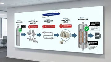
Purity at Point-of-Use, Not Just at the Cylinder
Gas purity at the cylinder means nothing if contamination enters downstream. Every component between the cylinder and the process tool is a potential source of contamination:
- Regulators, manifolds, and valves introduce moisture and oxygen at fitting interfaces
- Unpassivated lines contribute hydrocarbons and particulates
- Residual outgassing from elastomers and seals compounds over time
Point-of-use (POU) purifiers — heated getters and cryogenic adsorbers — remove H₂O, O₂, and hydrocarbons down to sub-ppb levels. Without them, even 6N-certified gas can arrive contaminated at the process tool.
NIST-Traceable Calibration Standards for Process Monitoring
Process control sensors inside fabs must themselves be calibrated with verified reference gas standards to ensure measurements governing process quality are accurate. Gas certificates of analysis must comply with ISO 6141. Calibration itself relies on NIST Standard Reference Materials (SRMs) and NIST Traceable Reference Materials (NTRMs) to establish metrological traceability back to a primary standard.
SpecGas Inc. produces NIST-traceable rare gas blend standards — including neon, krypton, and xenon mixtures — blended in-house using proprietary cylinder treatment processes developed to maintain stability at low ppm and ppb concentration levels.
Supply Chain Risks and Sourcing Noble Gases Reliably
Geographic Concentration Creates Single-Point-of-Failure Risk
Neon, krypton, and xenon are extracted as byproducts from Air Separation Units (ASUs) that produce oxygen for steel mills. Only the largest ASUs—processing over 1,000 tons of oxygen per day—can economically extract these trace gases. Historically, these large ASUs were concentrated in Ukraine and Russia due to the Soviet steel industry's scale. This geographic concentration created severe supply vulnerability.
Post-2022 Mitigation Strategies
The 2022 Ukraine conflict forced the semiconductor industry to adopt aggressive mitigation strategies:
- Gas Recycling Systems: EFC Gases launched a Cymer-qualified Neon Gas Recycling System that captures spent neon from laser exhausts, reconditions it to spec, and guarantees stable pricing while reducing carbon emissions.
- Geographic Diversification: Gas suppliers are building ASUs outside Eastern Europe. Air Liquide is constructing a large-scale ASU in Naoshima, Japan, to co-produce argon and neon for regional semiconductor customers.
- Strategic Stockpiling: Chipmakers have increased safety stocks of noble gases to buffer against future geopolitical disruptions.
Choosing the Right Specialty Gas Partner
These supply chain lessons translate directly into what process engineers and procurement managers should demand from their gas suppliers. The differentiators that matter most:
- Requires NIST-traceable purity certification so measurements are accurate and auditable
- Delivers batch-to-batch consistency through controlled blending — composition drift in noble gas mixtures directly degrades laser performance
- Maintains reliable lead times to prevent the fab downtime that commodity supply shortages caused in 2022
- Produces non-standard mixtures and rare gas blends that large commodity suppliers frequently deprioritize or decline
Specialty suppliers like SpecGas Inc. offer a cost-effective alternative to commodity gas companies for rare and reactive noble gas mixtures. With all blends produced in-house and lead times far shorter than larger suppliers, SpecGas fills orders that commodity distributors routinely turn away.
SpecGas's proprietary cylinder treatment process extends shelf life stability for reactive and rare gas mixtures — reducing concentration drift risk and ensuring consistent performance in semiconductor process environments.
Frequently Asked Questions
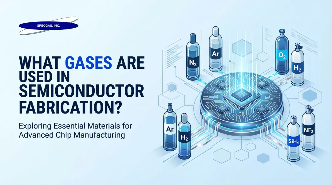
What noble gases are used in semiconductor manufacturing?
Five noble gases see active use in semiconductor fabs:
- Argon — primary plasma and sputtering medium
- Helium — wafer cooling and heat transfer
- Neon — essential for ArF excimer lasers in photolithography
- Krypton — advanced lithography and specialty ion implantation
- Xenon — high-power ion implantation and emerging EUV applications
What are semiconductor-grade gases?
Semiconductor-grade gases meet ultra-high purity (UHP) specifications, typically 99.9999% (6N) purity or higher, with impurities controlled at the parts-per-billion level. Certification and NIST traceability are required to ensure process consistency and device yield.
What are the 4 major stages of semiconductor processing?
The four stages are:
- Wafer fabrication — thin film deposition onto the silicon substrate
- Patterning/lithography — transferring circuit designs onto the wafer
- Etching — removing unwanted material to define structures
- Doping/ion implantation — introducing impurities to modify electrical properties
Noble gases contribute to each stage, from inert blanket gases during deposition to plasma media in etching and implant beamlines.
Do noble gases make good semiconductors?
No, noble gases themselves do not function as semiconductors. They are used as inert process gases, carrier gases, and plasma media within semiconductor manufacturing equipment—not as semiconductor materials themselves.
How rare is xenon?
Xenon exists in Earth's atmosphere at approximately 0.09 parts per million by volume, making it one of the rarest stable gases. That scarcity drives its high cost and creates real supply chain pressure for fabs that depend on it.
What are the 7 noble gases?
The seven Group 18 elements are helium, neon, argon, krypton, xenon, radon, and oganesson. Radon is radioactive with no industrial utility, and oganesson is a short-lived synthetic element — leaving five stable, commercially viable gases for industrial use.