Introduction
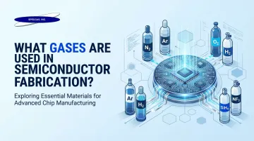
Modern semiconductor chips power everything from smartphones to electric vehicles — and producing them requires over 30 distinct process gases across fabrication stages. At nanometer-scale feature sizes, gas selection, purity, and consistency matter as much as the equipment itself. Even parts-per-billion (ppb) contamination levels can trigger device defects and costly yield loss.
Inside the fab, fabrication moves through a complex sequence — deposition, lithography, etching, doping, and cleaning — with each stage relying on gases chosen for their specific reactivity, inertness, or thermal properties. The global semiconductor gases market, projected to reach $10.9 billion in 2026, reflects just how critical these materials have become.
This article breaks down the five core gas categories used in chip production: deposition, etching, dopant, carrier/inert, and cleaning gases. You'll learn why Ultra-High Purity (UHP) standards are essential and what to look for in a reliable specialty gas supply partner.
Key Takeaways
- Semiconductor fabs rely on five gas categories—deposition, etching, dopant, carrier/inert, and cleaning—each performing a distinct role in building and shaping circuits
- Nitrogen, argon, and helium consumption is massive—modern fabs use up to 50,000 cubic meters of nitrogen per hour
- Ultra-High Purity (6N/99.9999% or higher) is essential—ppb-level impurities directly impact yield
- Toxic process gases like arsine, phosphine, and hydrogen chloride require precise concentration control—even small deviations alter device electrical properties
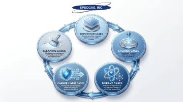
How Gases Are Categorized in Semiconductor Fabrication
The semiconductor fabrication process involves a layered sequence of steps—deposition, lithography, etching, doping, and cleaning—with gases purpose-selected for each step based on their chemical reactivity, inertness, or thermal properties.
Gases fall into five main functional categories:
- Deposition gases — Build thin films layer by layer through chemical vapor deposition (CVD)
- Etching gases — Selectively remove material to transfer circuit patterns onto wafers
- Dopant gases — Modify electrical conductivity by introducing impurity atoms
- Carrier/inert gases — Protect wafers, transport reactive gases, and support plasma environments
- Cleaning gases — Remove residues and deposits to maintain process consistency
These categories aren't always rigid. Gases like ammonia, oxygen, and boron trichloride appear across multiple categories depending on concentration and application. The NIST Index of Semiconductor Process Gases lists over 30 distinct gases used in chip manufacturing—a range that reflects how chemically diverse modern fab processes have become.
Deposition Gases: Building Thin Films Layer by Layer
Chemical vapor deposition (CVD) uses gases that react or decompose on wafer surfaces to deposit uniform layers of material—oxides, nitrides, metals—that form the functional layers of a chip.
Silane and Germane
Silane (SiH₄) is the primary precursor for depositing silicon-based films in CVD processes. It decomposes at high temperatures, liberating hydrogen and leaving pure silicon on the wafer surface, making it fundamental to transistor and gate oxide formation.
Germane (GeH₄) serves as the germanium-equivalent precursor for silicon-germanium (SiGe) layers in high-speed devices. Incorporating germanium increases hole mobility, with research demonstrating hole effective mobility of 480 cm²/Vs in strained Si pMOSFETs formed on SiGe structures—a meaningful gain for high-speed, low-power transistor designs.
Ammonia and Tungsten Hexafluoride
Ammonia (NH₃) combines with silane in plasma-enhanced CVD (PECVD) to deposit silicon nitride (Si₃N₄) films—the most common nitrogen source for these dielectric and barrier layers critical to chip architecture. Silicon nitride appears throughout modern devices as an insulator, diffusion barrier, and etch stop.
Tungsten hexafluoride (WF₆) is the dominant precursor for tungsten CVD due to its low cost, high purity, and high vapor pressure enabling efficient deposition rates. It is reduced with hydrogen or silane to deposit tungsten metal, valued for low resistivity and resistance to electromigration in interconnects.
Additional specialty gases extend deposition capability for next-generation device structures:
- Germanium tetrafluoride (GeF₄): used in ion implantation for germanium doping
- Molybdenum hexafluoride (MoF₆): enables atomic layer deposition of MoSiₓ films in advanced node architectures
Etching Gases: Patterning with Precision
Etching uses reactive gases in plasma systems to selectively remove material and transfer circuit patterns from photomasks onto wafers. Plasma etching enables anisotropic (directional) precision needed for modern sub-10 nm nodes, contrasting with isotropic (all-direction) wet chemical methods.
Fluorine-Based Etching Gases
Sulfur hexafluoride (SF₆) is widely used for Deep Reactive Ion Etching (DRIE) in the Bosch process, alternating between SF₆ etch steps and passivation steps to create high-aspect-ratio structures like Through-Silicon Vias (TSVs) and MEMS devices.
Carbon tetrafluoride (CF₄) is common for etching silicon dioxide (SiO₂) and silicon nitride (SiNₓ) due to its strong fluorine content. It also serves dual duty in CVD chamber cleaning applications.
Pure fluorine (F₂) and fluorine/nitrogen mixtures enable precise, selective material removal in plasma etching. Phosphorus trifluoride (PF₃) is increasingly used as a lower global warming potential (GWP) substitute in applications where SF₆ or CF₄ would otherwise be specified.
Chlorine-Based Etching Gases
Chlorine-based gases handle metal and compound semiconductor etching where fluorine chemistry falls short:
- Chlorine (Cl₂) etches aluminum, tungsten, GaAs, and GaN with strong anisotropy
- Boron trichloride (BCl₃) removes native oxide layers like Al₂O₃ and delivers smoother etch profiles than pure Cl₂; it also functions as a p-type dopant source, making it a cross-category gas
- Hydrogen bromide (HBr) provides highly selective, anisotropic etching of polysilicon gates — HBr-based plasmas can achieve near-infinite selectivity to underlying gate oxides, which is critical for preserving delicate device structures
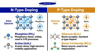
Dopant Gases: Engineering Electrical Properties
Doping intentionally introduces impurity atoms into semiconductor material to modify its electrical conductivity. N-type doping adds electron donors (phosphorus, arsenic), while p-type doping adds electron acceptors (boron). Precise dopant gas concentration is critical—variations directly impact transistor threshold voltages and device performance. The three gases below cover the most widely used dopant sources in silicon and III-V semiconductor production.
Key Dopant Gases
Phosphine (PH₃) is the primary n-type dopant gas, introducing phosphorus into silicon. Toxic and flammable, it requires precise handling and containment throughout delivery and use. For calibration and bump testing applications, phosphine is available in concentrations from 300 ppb to 5%—SpecGas Inc. uses a proprietary cylinder treatment process to ensure optimal stability and extended shelf life for these reactive mixtures.
An arsenic dopant source used in both transistor manufacturing and III-V compound semiconductor production, arsine (AsH₃) is among the most hazardous gases in fabrication. The OSHA Permissible Exposure Limit is 0.05 ppm (8-hour TWA), making tightly controlled delivery systems and rigorous safety protocols non-negotiable.
For p-type doping, fabs rely on diborane (B₂H₆) and boron trichloride (BCl₃). Diborane is thermally unstable, decomposing at room temperature, and requires dilution in hydrogen (typically 10%) for safe delivery. BCl₃ offers a more stable alternative, serving dual roles in p-type doping and chlorine-based plasma etching processes.
Inert, Carrier, and Cleaning Gases: Keeping the Process Stable
Inert and carrier gases don't participate in chemical reactions — but they're essential to keeping fabrication stable. Their roles include:
- Protecting wafers from contamination by oxygen and moisture
- Carrying reactive gases into process chambers
- Supporting and sustaining plasma environments
- Purging lines between process steps
Nitrogen, Argon, and Helium
Nitrogen (N₂) is the highest-volume gas in semiconductor fabs: used for purging pipelines, inerting process chambers, and preventing reactive oxygen or moisture from reaching sensitive wafers. Modern fabs can consume up to 50,000 cubic meters of nitrogen per hour.
Argon (Ar) serves as the preferred plasma gas for sputtering (physical vapor deposition) and ion implantation. Its low ionization energy produces stable, controllable plasma, and complete inertness eliminates the metal-nitride contamination risk that nitrogen can introduce.
Helium (He) is used for wafer backside cooling on electrostatic chucks. Typical backside gas pressures range from 2 to 20 Torr, protecting wafers from thermal damage during high-energy processes. It also serves as the standard tracer gas for mass spectrometry leak detection in vacuum chambers and gas delivery systems — a role that relies on its low atomic mass and chemical inertness.
Cleaning Gases
Cleaning gases remove chamber deposits and surface residues between wafer runs, maintaining process consistency without breaking vacuum unnecessarily.
| Gas | Method | Primary Use |
|---|---|---|
| O₂ | Plasma cleaning | Oxidizes and removes organic residues and photoresist after processing |
| NF₃ | Remote Plasma Cleaning (RPC) | Generates fluorine radicals at >99% source gas destruction to clear silicon-based CVD chamber deposits |
| ClF₃ | Vapor-phase cleaning | Cleans CVD chambers without plasma or elevated temperatures; requires stringent safety handling due to extreme reactivity |
Note: NF₃ and SF₆ have extremely high Global Warming Potentials (16,100 and 23,500 respectively), requiring strict abatement systems and ongoing process optimization.
Why Ultra-High Purity and Reliable Gas Supply Matter
Semiconductor processes operate at nanometer-scale feature sizes where even ppb-level impurities—oxygen, moisture, hydrocarbons—can cause device defects, reduced yield, and costly process failures. Gases used in fabs typically must meet Ultra-High Purity (UHP) or "electronic grade" specifications with purity levels of 99.9999% (6N) or better.
UHP specifications by example:
- Matheson ULSI 6N Argon: 99.9999% purity with O₂ ≤300 ppbv, H₂O ≤500 ppbv
- PurityPlus Grade 7.0 Helium: 99.99999% purity with O₂ <50 ppb, H₂O <20 ppb
As process nodes shrink (7 nm to 5 nm and beyond), moisture levels must be reduced to 15 ppbV or less to prevent corrosion in gas delivery systems. Metal contaminants must be reduced to <10⁸ atoms/cm² to prevent gate stack degradation.
Beyond raw purity, consistency of gas mixture composition across every cylinder or supply run is just as critical. Variability in dopant gas concentration or etchant ratios directly impacts device uniformity and production yield. Precision specialty gas blending and NIST-traceable calibration standards are what close that gap.
When evaluating gas suppliers for semiconductor applications, look for:
- NIST-traceable calibration standards with documented gravimetric accuracy
- Proven shelf stability for reactive mixtures (phosphine, arsine, chlorine-based blends)
- Ability to produce ppb-level precision blends, not just standard concentrations
- Proprietary cylinder treatment processes that preserve reactive gas integrity over time
SpecGas Inc. specializes in exactly these requirements — producing NIST-traceable gas standards with a proprietary cylinder treatment process and Stability Guarantee for reactive mixtures, including dopant gases from 300 ppb to 5% concentration. For fabs where standard suppliers fall short on unusual formulations or tight lead times, that kind of specialty depth makes a practical difference.
Frequently Asked Questions
What gases are used in semiconductor chip manufacturing?
Semiconductor fabrication relies on five core categories: deposition gases (silane, germane, ammonia, WF₆), etching gases (SF₆, CF₄, Cl₂, HBr), dopant gases (phosphine, arsine, diborane), inert/carrier gases (nitrogen, argon, helium), and cleaning gases (oxygen, NF₃, ClF₃). A modern fab typically draws from 30 or more distinct gases across these groups.
What are electronic gases used in semiconductor manufacturing?
"Electronic gases" refers to high-purity specialty gases used in chip production — both bulk gases (nitrogen, argon, helium, hydrogen) and process gases (silane, phosphine, SF₆, NF₃) — all meeting purity specs of 99.9999% (6N) or higher with impurities controlled at ppb levels.
Which inert gases are used in semiconductor chip manufacturing?
Nitrogen, argon, and helium are the primary inert/noble gases. Nitrogen is used for purging and inerting (up to 50,000 m³/h consumption), argon for plasma environments and sputtering due to its low ionization energy, and helium for thermal management (wafer cooling) and leak detection in gas delivery systems.
Why is ultra-high purity (UHP) important for semiconductor gases?
At nanometer-scale feature sizes, even ppb-level impurities like oxygen or moisture cause device defects, reduce yield, and degrade performance. Moisture above 15 ppbV can corrode gas lines; metal contaminants above 10⁸ atoms/cm² degrade gate oxides. UHP grades (99.9999% and above) with NIST-traceable standards are required to hold these thresholds.
What is the difference between process gases and bulk gases in semiconductor manufacturing?
Bulk gases (nitrogen, argon, helium, hydrogen) are used in large volumes for purging, inerting, and plasma environments—often consumed continuously throughout fab operations. Process gases (silane, phosphine, SF₆, NF₃) are specialty gases used in smaller quantities for specific chemical reactions like deposition, etching, and doping, requiring higher purity and more precise control.