Introduction
At process geometries below 10 nm, a particle only tens of nanometers in diameter acts as a "boulder" relative to circuit features—causing open circuits, bridging failures, line width variation, and wafer scrap. According to the 2024 IRDS Yield Enhancement report, 3.5 nm is now the smallest critical particle size for advanced logic devices.
That threshold exposes a serious metrology gap: online particle counters cannot reliably detect below 20 nm, meaning most critical defects go undetected before they ruin wafers.
Since filtration is your primary defense against contamination that metrology can't catch, understanding it end-to-end matters.
This guide is for process engineers, fab facility managers, and electronics manufacturers. It covers how process gas filtration works, what it removes, how filter types differ, what governs performance, and where teams commonly get it wrong. We'll also explain why contamination control starts upstream—with high-purity, NIST-traceable source gases—and how filtration at every sequential point protects both your wafers and your process equipment.
TLDR
- Process gas filtration removes solid particles, moisture, and molecular contaminants from gases used in semiconductor manufacturing—preventing nanoscale defects that kill yield
- Filtration occurs at multiple sequential points: bulk gas source → distribution panels → valve manifold boxes → point of use at the process chamber
- SEMI industry standard requires at least 9-log particle reduction down to 0.003 µm; newer systems push this to 0.0015 µm
- Sintered metal and ceramic filters offer depth filtration and durability; PTFE membrane filters are chemically compatible but prone to failure under purge cycling
- Source gas purity, filter media selection, operating pressure, and purge cycling behavior drive filtration system effectiveness
What Is Process Gas Filtration?
Process gas filtration is the engineered removal of contaminants—particles, metallic ions, moisture, hydrocarbons, and other molecular impurities—from specialty gases used at every stage of semiconductor fabrication, from thin film deposition to etching and lithography.
The goal is to deliver gas to the process chamber at ultra-high purity (99.999% or greater), ensuring no contaminant reaches the wafer surface and disrupts the atomic-scale precision of modern chip manufacturing.
Filtration vs. Purification:
Process gas filtration and gas purification are related but distinct steps:
- Filtration targets solid particles and aerosols using physical media—sintered metal, PTFE, ceramic—that physically trap or sieve contaminants
- Purification targets molecular-level impurities like H₂O, O₂, and CO using adsorption materials such as molecular sieves or catalytic beds
Both are often deployed together in sequence within the same gas line, but they are distinct steps with different mechanisms. Understanding which step addresses which contaminant type is the first decision in designing a semiconductor gas delivery system.
Why Process Gas Filtration Is Critical in Semiconductor Manufacturing
Modern semiconductor nodes operate at a contamination sensitivity that defies everyday intuition. At process geometries below 10 nm, even particles tens of nanometers in diameter cause fatal defects—open circuits, bridging failures, line width variation, and complete wafer scrap.
Types of Contaminants and Their Sources
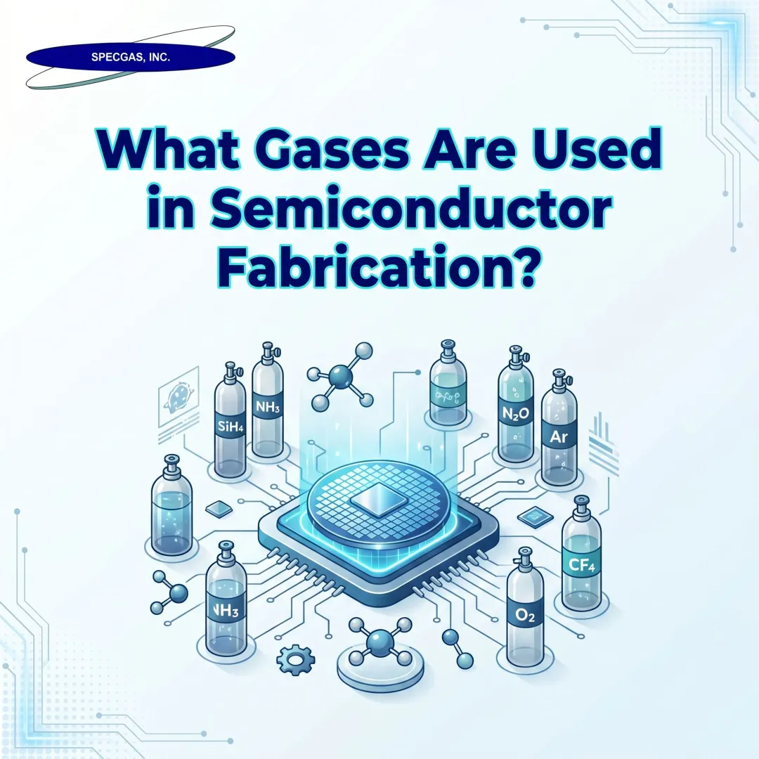
Process gases carry multiple categories of contaminants that filtration must remove:
- Solid particles shed from cylinder valves, pipelines, and welds during gas distribution
- Metal ions (Fe, Ni, Cr, Ti) from system components that can contaminate films
- Molecular contaminants including H₂O, O₂, hydrocarbons, and siloxanes
- Chemical by-products from reactive gas interactions within the delivery system itself
What Happens Without Adequate Filtration
The consequences vary by process but are severe:
- CVD/ALD processes suffer film stoichiometry shifts when molecular impurities enter the reaction zone, destroying device performance
- Etching: Particles create defect points in patterned features, ruining critical dimensions
- Lithography: Moisture or organic contamination interferes with photochemical reactions, destroying pattern fidelity
SEMI Standards and System Design Requirements
SEMI standards mandate specific log-reduction performance for process gas filtration. Filtration is embedded at multiple required points throughout every properly designed UHP gas delivery system — it is a design requirement, not an add-on.
How Source Gas Purity Reduces Filter Load
Filtration effectiveness depends partly on what enters the system in the first place. Reactive gas mixtures like Cl₂, phosphine, or silane that arrive with verified purity and documented stability place a lower burden on downstream filters — reducing breakthrough risk and extending service life.
SpecGas supplies NIST-traceable specialty gas blends for semiconductor applications, including reactive mixtures prepared with a proprietary internal cylinder treatment that prevents wall reactions during storage. Starting with a well-characterized source gas means your filtration system works with the chemistry it was designed for, rather than compensating for upstream variability.
How Process Gas Filtration Works
Process gas moves from bulk supply or cylinder through a sequential chain of filtration stages, each targeting specific contaminant types and sizes. The strictest filtration requirements are concentrated at the point closest to the wafer, where even sub-nanometer particles can kill yield.
Two Dominant Filtration Mechanisms:
- Depth filtration (sintered metal/ceramic): Uses sieving, impaction, diffusion, surface attraction, and entrapment across a thick, tortuous matrix—achieving 9-log reduction (99.9999999% removal)
- Surface filtration (PTFE/membrane): Uses a thin sieve layer to strain particles by size—effective when intact but vulnerable to tearing under differential pressure spikes during purge cycling
Gas Purifiers as a Complementary Stage:
Where molecular impurities (H₂O, O₂, hydrocarbons, NH₃) must be reduced to ppb or ppt levels, adsorption-based purifiers using metal oxides, activated copper, or molecular sieves are installed—often in series with particulate filters within the same gas line.
Step 1: Bulk Source and Cylinder Outlet Filtration
The first filter intercepts particles shed from the cylinder valve, cylinder interior, and transport contamination before gas enters the distribution system. This stage uses a sintered metal element rated for the full delivery pressure of the cylinder. Cylinder treatment processes that minimize wall reactions and particle shedding — such as those used by SpecGas — directly reduce the contamination load this first filter must handle.
Step 2: Distribution Panel and Gas Cabinet Filtration
Filters at the manifold inlet, valve manifold boxes (VMBs), and gas cabinets protect downstream components from particle damage. Unfiltered gas damages sensitive MFCs and pressure regulators, which then become secondary particle generators. Once those components degrade, contamination originates from inside the delivery system — not just the source. That distinction is what drives the tighter filter ratings required at the next stage.
Step 3: Point-of-Use (POU) Filtration at the Process Chamber
The final filtration stage immediately before gases enter the ALD, CVD, etch, or diffusion chamber is the most particle-sensitive location in the entire gas delivery chain. 0.0015 µm-rated UHP filters are required here. Particles generated by valve actuation, line vibration, or fitting wear between the last upstream filter and the chamber face no additional barrier — making POU filter integrity the last line of defense against yield loss at the wafer surface.

Key Factors That Affect Process Gas Filtration in Semiconductor Manufacturing
Source Gas Quality
The initial purity grade of the process gas is one of the most impactful variables in filtration system design. A gas sourced from a NIST-traceable certified specialty gas supplier arrives with a documented, stable composition, which reduces unexpected contaminant spikes that would overwhelm filters. Reactive gas mixtures with poor shelf-life stability can also introduce particulate from cylinder wall reactions, making both source gas quality and cylinder treatment critical upstream considerations.
Filter Media and Chemical Compatibility
Sintered stainless steel, Hastelloy, nickel, and inert alumina ceramics each have different compatibility profiles with corrosive process gases:
| Material | Best For | Avoid For |
|---|---|---|
| 316L Stainless Steel | Inert gases, general applications | Cl₂, HCl, HBr — susceptible to chloride-induced pitting |
| Hastelloy C-22/C-276 | Aggressive halogen/halide etchants | Cost-sensitive applications |
| PTFE | Broad chemical compatibility | High differential pressure cycling |
| Alumina Ceramic | High-temperature, corrosive gases | Mechanical shock environments |

Selecting a filter material incompatible with the gas chemistry risks corrosion of the element, particle generation from within the filter itself, and catastrophic filtration failure.
Operating Conditions: Pressure, Temperature, and Purge Cycling
High differential pressure events during cycle purging are the leading cause of PTFE membrane filter element failure, tearing or perforating the thin sieve layer. Sintered monolithic elements withstand repeated purge cycles without structural degradation, and Hastelloy variants handle elevated process temperatures. Conventional filter media may degrade during heated dry-down cycles used to remove residual moisture between process steps.
Filtration Rating and Particle Size Targets
As process nodes shrink, the particle sizes that cause yield-killing defects also shrink. A particle 3 nm in diameter that was inconsequential in a 500 nm process is a fatal defect in a 7 nm node. Filter ratings must be matched to the current and planned node geometry, not just to historical standards.
Common Issues and Misconceptions About Process Gas Filtration
Misconception 1: No Visible Failure Means the Filter Is Working
The most common and costly misconception is that PTFE membrane filters are functioning because there is no visible indication of failure and no pressure differential increase. After repeated purge cycle events, the thin PTFE membrane can tear or perforate—creating a path of least resistance through which particles pass unfiltered. The welded-shut stainless housing prevents visual inspection without cutting it open. Experienced engineers who have had housings cut open after service have confirmed this failure mode; many active engineers are unaware of it.

Misconception 2: Low Pressure Drop Signals Good Performance
The low ΔP of membrane filters is often interpreted as a sign of efficiency, when in fact it may indicate the element has failed and gas is bypassing the damaged media entirely. A properly functioning sintered depth filter has a measurably higher ΔP—which is a feature, not a flaw, as it confirms the filter is actively working.
Misconception 3: Fixed Schedules and Single Filters Are Enough
Filters are frequently changed on fixed calendar schedules rather than based on actual contamination loading, process conditions, or verified performance. Teams that skip post-service element inspection (for example, cutting used elements cut open) are operating on assumptions.
Two common gaps that compound this problem:
- A single upstream filter does not eliminate the need for point-of-use filtration — particles can be generated within the gas line itself between filtration stages
- Used filter elements are rarely inspected after removal, leaving teams with no feedback on actual contamination levels or failure modes
Conclusion
Process gas filtration is the systematic, multi-stage removal of contaminants from semiconductor process gases, protecting wafer surfaces from particle defects and molecular contamination at every point from the gas source to the process chamber.
For engineers and procurement teams, effective gas filtration comes down to four practical decisions:
- Select filter media matched to the specific gas chemistry in use
- Match filtration rating to the process node requirements
- Understand the real-world failure modes of each filter type before deployment
- Treat upstream gas purity as a variable in contamination control strategy, not a fixed assumption
Starting with NIST-traceable source gases from suppliers like SpecGas — which use proprietary cylinder treatments to minimize contamination at the origin — reduces the burden on downstream filtration and lowers the risk of breakthrough events that compromise yield.
Frequently Asked Questions
What is the difference between process gas filtration and gas purification in semiconductor manufacturing?
Filtration physically removes solid particles and aerosols using porous media (sintered metal, PTFE, ceramic), while purification removes molecular-level impurities (H₂O, O₂, hydrocarbons) using adsorption materials. Both are commonly deployed in series on the same gas line, but they target entirely different contaminant types.
What purity level is required for gases used in semiconductor manufacturing?
Semiconductor process gases generally require 99.999% (5N) purity or higher, measuring molecular impurities at ppb or ppt levels for advanced nodes. At sub-10 nm geometries, even trace moisture or oxygen at ppm concentrations can alter film properties or cause defects.
What is a 9-log particle reduction in the context of semiconductor gas filtration?
9-log reduction means the filter removes 99.9999999% of particles at or above its rated size—so if one billion qualifying particles entered the filter, only one would pass through. SEMI uses this as the standard for UHP gas filtration, and advanced sintered metal filters are now rated down to 0.0015 µm particle sizes.
Why do PTFE membrane filters fail in semiconductor process gas lines?
PTFE membrane filters use a thin sieve layer that can tear or perforate when subjected to high differential pressure spikes during cycle purging. Once damaged, the torn area becomes the path of least resistance, allowing particles to bypass the filter entirely—often with no visible warning to operators.
How many gas filters are typically installed on a single gas line in a semiconductor fab?
A properly designed UHP gas delivery system installs filters at multiple critical nodes: at the bulk source, at the gas distribution panel, at the gas drop to the process tool, inside the tool's gas box, and at the process chamber inlet. Some OEMs add additional filters between the gas box and chamber.
Which filter material is best for corrosive semiconductor process gases like Cl₂ or HF?
Hastelloy-based sintered metal elements offer superior corrosion resistance for aggressive halide and acid-based gases compared to standard stainless steel or PTFE. Material selection must be validated against the specific gas chemistry, concentration, and operating temperature to avoid filter degradation that would introduce particles into the process.