Introduction
Helium rarely dominates semiconductor procurement discussions—until it's missing. This unassuming gas touches nearly every critical stage of chip fabrication, from photolithography to wafer cooling to plasma etching.
A March 2026 supply shock made this concrete: attacks on Qatar's Ras Laffan complex knocked out 27–30% of global helium supply, causing spot prices to surge 40–100% within weeks and forcing fabs into painful allocation decisions.
Most procurement teams don't feel helium's importance until a disruption forces the conversation. By then, the damage is already underway — unplanned fab downtime costs between $1 million and $3.8 million per hour, making stock-outs financially devastating.
Understanding exactly where helium fits into fab operations — and what breaks without it — is the first step toward sourcing it reliably. This article covers the specific functions helium performs, what those functions cost when compromised, and what dependable supply actually requires.
Key Takeaways
- Helium's unique properties—chemical inertness, highest thermal conductivity of any gas, and exceptionally small atomic radius—make it irreplaceable across multiple semiconductor fabrication stages
- Three fabrication functions have no viable substitute: wafer cooling on electrostatic chucks, atmosphere control in process chambers, and carrier gas for lithography and etching
- Semiconductors already consume 24% of global helium supply—projected to hit 30% by 2030 and grow fivefold by 2035
- Supply inconsistency or purity deviations drive higher defect rates, reduced yield, and unplanned downtime—not just cost increases
- Sourcing high-purity helium from a qualified specialty gas provider protects yield, uptime, and process consistency at every fabrication stage
What Is Helium's Role in Semiconductor Manufacturing
Helium is not a raw material that becomes part of the chip. It is a process gas that enables the conditions under which chips can be made correctly, consistently, and at scale.
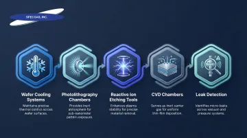
Helium appears throughout the fab:
- Wafer cooling systems – Maintains precise temperature during plasma processes
- Photolithography chambers – Purges oxygen and moisture in EUV and DUV tools
- Reactive ion etching tools – Controls plasma density and etch selectivity
- Chemical vapor deposition chambers – Carries reactive gases across wafer surfaces
- Leak detection for process equipment – Mass spectrometer scans to qualify vacuum chambers
Because helium is used throughout the process rather than at one isolated step, a supply disruption or purity drop doesn't affect a single tool—it introduces quality and throughput risks at every stage of the fabrication line simultaneously.
Unlike bulk chemicals, helium cannot be safely stockpiled in large quantities at the fab level. Most fabs maintain only about one week of on-site inventory, which means procurement gaps translate directly into production stops—not slowdowns.
Key Roles Helium Plays in the Fab: Why It Cannot Be Replaced
Helium's value in the fab comes down to physical properties no other gas can replicate at the temperatures, pressures, and tolerances advanced semiconductor fabrication requires. The three roles below each connect directly to measurable outcomes: yield rate, defect density, thermal stability, and process integrity.
Thermal Management and Wafer Cooling
Helium serves as a backside cooling gas on electrostatic chucks (ESCs) to maintain precise wafer temperature during plasma etching, ion implantation, and deposition—processes that generate significant localized heat at nanometer-scale features. A microscopically thin layer of helium is injected between the silicon wafer and the chuck, acting as a thermal bridge to transfer heat away from the wafer surface.
Why this works: Helium has exceptionally high thermal conductivity of 156.7 mW/m·K at 300 K, second only to hydrogen. This allows it to transfer heat efficiently even at very low pressures, keeping temperature uniformity within the tight tolerances required for sub-10nm node production.
Impact on yield: Uneven wafer temperature during etching or deposition directly causes pattern distortion, critical dimension variation, and die failure. Thermal-induced yield loss destroys profit margins, especially given the astronomical costs of advanced node wafers:
| Node | Foundry | Avg Wafer Cost (2026) |
|---|---|---|
| 3nm | TSMC N3/N3E | $19,500 |
| 5nm | TSMC N5/N4 | $18,500 |
| 7nm | TSMC N7 | $9,500 |
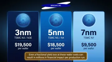
With 3nm wafers costing up to $19,500 to produce, even a fractional percentage improvement in defect rate translates to significant cost-per-good-die impact.
KPIs impacted:
- Wafer yield rate
- Critical dimension uniformity
- Defect density per wafer
- Cost per good die
When this matters most: Thermal management becomes increasingly critical at advanced nodes (sub-7nm and below) and in high-volume DRAM and logic production where wafer costs are highest and tolerance bands are narrowest.
Inert Atmosphere for Contamination-Free Fabrication
Helium's complete chemical inertness—it does not react with silicon, photoresists, process gases, or any fab material at standard operating conditions—makes it the preferred purging and atmosphere gas for sensitive process chambers.
Fabs use helium to purge tools between runs, displace reactive or moisture-bearing gases, and maintain clean environments where even trace oxygen or water vapor would cause oxidation or defect formation on wafer surfaces.
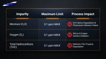
Why this is critical: Semiconductor fabrication at advanced nodes operates with contamination tolerances measured in parts per billion. A single reactive gas molecule in the wrong place can cause a localized defect that kills a die. Fabs require 6N grade helium (99.9999% purity), with strict limits on critical contaminants:
| Impurity | Maximum Limit | Impact |
|---|---|---|
| Moisture (H₂O) | < 0.1 ppm | Fogs EUV optics; photoresist adhesion failures |
| Oxygen (O₂) | < 0.1 ppm | Oxidizes silicon/copper surfaces; barrier layer defects |
| Total Hydrocarbons | < 0.1 ppm | Degrades dielectric film properties |
In EUV optics, if hydrocarbon contamination exceeds critical thresholds, carbon deposition reduces mirror reflectance by around 1.6%, demanding surface cleaning that causes severe downtime.
Operational impact: Contamination events don't just affect the wafer in process—they trigger tool downtime, cleaning cycles, and requalification runs that cost hours or days of production time.
KPIs impacted:
- Particle counts per wafer
- Tool uptime
- Contamination event frequency
- Requalification downtime
When this matters most: Contamination control is most critical during EUV lithography and ALD (atomic layer deposition) processes, where sub-nanometer-scale material interactions are involved and process chamber conditions are most sensitive to gas impurities.
Carrier and Process Gas in Photolithography and Plasma Etching
In EUV and DUV photolithography, helium functions as a carrier and purge gas inside optical columns and reticle pods. Its transparency to UV wavelengths with minimal absorption and scattering enables the precise light delivery that defines circuit patterns on silicon at nanometer scale.
In plasma etching, helium serves a separate but equally precise role: as a diluent gas that stabilizes and controls plasma density and energy distribution across the wafer surface.
Why helium is unique: EUV lithography uses 13.5 nm light to print features on silicon wafers. Because EUV light is absorbed by almost everything, including air, the optical path must be kept in a highly controlled environment. Even small concentrations of other gases would absorb the extreme UV light before it reaches the wafer—helium's transparency to EUV radiation makes it the only gas compatible with the optical path.
Scale of dependency: ASML has shipped its first High-NA EUV lithography systems to Intel, Samsung, and SK Hynix, with systems capable of processing 175 wafers per hour. As nodes shrink to 2nm and High-NA EUV is adopted, helium consumption per wafer increases to an estimated 0.471 m³ per wafer—a 1.20x relative intensity compared to 3nm due to the multiplication of process steps and continuous purges.
No viable substitute exists: No alternative gas combines EUV transparency with chemical inertness—this is a physical constraint, not an engineering preference. EUV lithography is the foundational process for sub-7nm chips powering AI accelerators, advanced memory, and high-performance computing. There is no path to those chips without helium.
KPIs impacted:
- Lithographic resolution
- Pattern placement accuracy
- Plasma uniformity
- Etch selectivity
When High-NA EUV arrives: This dependency grows more pronounced as nodes shrink. The transition to High-NA EUV and multi-patterning techniques at leading-edge fabs increases helium consumption per wafer with each process generation.
What Happens When Helium Supply Is Disrupted or Impure
Semiconductor fabs typically maintain only days to weeks of on-site helium inventory. Unlike bulk chemicals, helium cannot be safely stockpiled in large quantities at the fab level, meaning continuous supply is an operational requirement rather than a logistical preference.
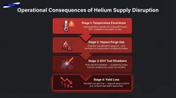
Direct operational consequences of helium shortage or purity deviation:
- Temperature excursions from cooling failures increase defect density and cause CD variation, cutting yield on every wafer processed during the disruption
- Impure purge gases trigger chamber qualification runs, unplanned tool downtime, and potential product hold events
- EUV lithography tools require controlled shutdown and restart sequences that consume engineering time and reduce utilization rates
- Yield losses spread fixed fab costs across fewer good die, driving up cost per chip
Helium disruptions rarely isolate to a single process step. Because helium runs across multiple tools simultaneously, a supply event creates bottlenecks at several points in the fabrication flow — making recovery slower than any single-tool downtime event.
During the March 2026 supply crisis, foundries were forced to triage limited helium supplies to their smallest, most advanced processing nodes (3nm/2nm) to protect their highest-margin products, delaying legacy node production.
South Korean memory giants and Taiwanese foundries were highly exposed, having sourced 55% and 69% of their helium from Gulf nations, respectively.
How Semiconductor Fabs Can Protect Their Helium Supply
Supply protection starts with treating helium as a strategic process input: one that requires the same supplier qualification rigor as any other critical process chemical, including documented purity specifications, NIST-traceable certification, and verified batch consistency.
Qualified Supplier Relationships with Documented Grade Specifications
Semiconductor-grade helium must meet strict purity thresholds—typically 6N (99.9999%) or higher. Working with a specialty gas supplier who can certify purity to NIST-traceable standards and provide consistent blends is the foundation of supply reliability.
SpecGas Inc. provides NIST-traceable specialty gas standards with lead times that consistently outpace industry norms, making them a qualified partner for semiconductor operations that cannot tolerate batch variation or supply gaps. Their proprietary blending techniques and batch-verified quality control ensure consistency for processes—such as EUV lithography or wafer cooling—where any shift in gas composition carries real consequences.
What to require from suppliers:
- NIST-traceable certification for every batch
- Documented purity specifications with contaminant limits
- Certificates of analysis with each shipment
- Verified compatibility with process equipment
Helium Reclamation and Recycling Systems
Fabs that implement closed-loop helium recovery—particularly from wafer cooling and chamber purge applications—can meaningfully reduce their exposure to supply fluctuations. Leading fabs routinely recycle more than 70% of their helium, with some advanced closed-loop systems capable of recovering 90% to 95% of helium used.
Technologies utilizing hollow fiber membranes and Pressure Swing Adsorption (PSA) are deployed to recapture and purify exhaust helium back to usable grades. This shift from a linear "consume-and-vent" model to a circular system decouples fabs from chronic global supply volatility.
Supplier Diversification and Contract Structure
Relying on a single helium source or spot market purchasing creates concentration risk. Fabs benefit from maintaining qualified secondary suppliers and establishing supply agreements that include priority allocation clauses.
U.S.-based fabs have some insulation from domestic production sources, but global supply chains remain fragile due to geographic concentration. When spot prices have surged 40–100% during past supply shocks, procurement strategies without built-in protections leave fabs exposed. Effective sourcing structures include:
- Multiple qualified suppliers with verified purity standards
- Contract terms that guarantee priority access during shortages
- Regular audits of supplier capacity and backup inventory
Securing high-purity helium is ultimately a yield protection measure. Inconsistent purity between batches introduces process variability that shows up in defect rates, not just in equipment logs.
Conclusion
Helium's role in semiconductor manufacturing comes down to physics. Its thermal conductivity, chemical inertness, EUV transparency, and atomic radius work together in ways no other gas can replicate—enabling wafer cooling, contamination control, and lithographic precision at the tolerances advanced nodes require.
As node sizes shrink and EUV adoption expands, helium demand per wafer is rising, not falling:
- A 2nm High-NA EUV wafer requires 1.2x more helium than a 3nm wafer
- The semiconductor industry's share of global helium consumption is projected to grow from 24% today to 30% by 2030
That trajectory puts supply reliability and gas purity directly in the critical path of fab performance.
Given that reality, fabs that treat helium as a strategic process input—with qualified suppliers, documented purity standards, and supply continuity plans—are better positioned to maintain yield and throughput as the industry pushes toward smaller nodes.
Frequently Asked Questions
How is helium used in semiconductor manufacturing?
Helium performs three primary functions in fabs: backside wafer cooling on electrostatic chucks to maintain precise temperature control, inert atmosphere and purging in process chambers to prevent contamination, and as a carrier/purge gas in EUV and DUV photolithography tools to enable light transmission through the optical path.
Is helium needed for semiconductor manufacturing?
Yes, helium is non-substitutable at current and next-generation node sizes. No alternative gas replicates its specific combination of thermal conductivity, chemical inertness, and EUV transparency — properties that are each essential for sub-7nm node processes including wafer cooling and photolithography.
Why do semiconductor companies like TSMC need helium?
Leading-edge fabs running EUV lithography for sub-7nm chips require helium throughout the optical path to prevent light absorption and in wafer temperature management to maintain critical dimension uniformity. As these fabs scale up advanced node production (some systems process up to 175 wafers per hour), helium consumption grows in direct proportion.
Why can't we manufacture helium?
Helium forms as a byproduct of radioactive decay of uranium and thorium in natural gas deposits, and is recovered via cryogenic distillation during LNG processing. It cannot be synthesized economically at laboratory or industrial scale, making it a strictly finite and depleting resource with no viable production alternative.
What purity of helium is required for semiconductor manufacturing?
Semiconductor-grade helium typically requires 6N (99.9999%) purity, with critical contaminants like oxygen, moisture, and total hydrocarbons restricted to below 0.1 ppm. Deviations in purity can introduce contamination or process variability that directly affects wafer yield by causing defects in photoresist adhesion, dielectric films, and EUV optics.
What happens to semiconductor production when helium supply is disrupted?
Fabs experience increased defect rates, reduced wafer yield, and tool downtime from chamber requalification events. Because helium runs through lithography, cooling, and chamber purging simultaneously, a supply disruption creates cascading bottlenecks across the line — not isolated failures — making recovery slower and more costly than a single-process outage.