Introduction
At 7nm nodes and below, a single parts-per-million impurity in a process gas can shift parametric yield enough to pull a product line into the red. Shrinking device geometries and rising fab costs mean every process input carries measurable weight — including hydrogen. Crystal defect tolerance at advanced nodes is effectively zero, and gas quality is one of the few variables that can be controlled precisely.
Most fab documentation treats hydrogen as a bulk process gas without explaining what it actually does at the process level. This article closes that gap by connecting hydrogen's chemical properties to the outcomes engineers and procurement teams track: yield rates, equipment uptime, process repeatability, and cost of ownership.
The focus here is operational, not theoretical. Understanding hydrogen's role in electronics manufacturing leads directly to better sourcing decisions, tighter process control, and fewer production surprises.
Key Takeaways
- Hydrogen is used across annealing, epitaxy, thin-film deposition, chemical stabilization, EUV lithography, and ion implantation
- Uniform heat transfer, precision chemical control during layer growth, and equipment protection are the core process advantages
- Sub-specification purity or inconsistent supply degrades yield, increases defects, and shortens tool service intervals
- Consistent purity and a quality-verified supplier are essential to maximizing yield and tool longevity
What Is Hydrogen's Role in Electronics Manufacturing?
Hydrogen (H₂) is classified as a bulk process gas in semiconductor fabs and is used across semiconductor, display, LED, and photovoltaic manufacturing. Two chemical properties make it indispensable: excellent heat transfer capability (thermal conductivity of 186.6 mW·m⁻¹·K⁻¹ at 300 K, compared to 26.0 for nitrogen and 17.7 for argon) and its efficiency as a reducing and etching agent.
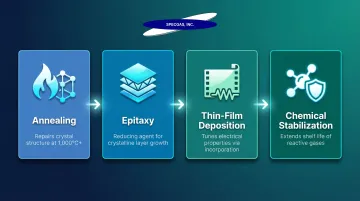
Four Established Applications
- Annealing: Repairs crystal structure at 1,000°C+ by transferring heat uniformly across wafers and reconstructing final crystal layers
- Epitaxy: Acts as a reducing agent for controlled crystalline layer growth on wafer surfaces
- Thin-film deposition: Controls film electrical properties by being incorporated into silicon films to increase resistivity and tune electronic behavior
- Chemical stabilization: Extends shelf life of reactive gases like diborane (B₂H₆) and digermane (Ge₂H₆)
Beyond these process staples, two newer applications are driving substantial hydrogen demand at leading-edge fabs — both tied directly to protecting expensive capital equipment.
Two High-Demand Emerging Applications
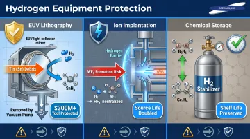
- EUV lithography — Reacts with tin deposits to form volatile stannane (SnH₄) for chamber cleaning, protecting collector optics that represent over $300 million in capital investment per tool
- Ion implantation — Blocks tungsten transport in ion sources by forming HFₓ instead of volatile tungsten hexafluoride (WF₆), doubling source life from 99 to 209 hours and reducing beam glitches by 50x
EUV tools alone consume hundreds of standard liters per minute per tool. That volume, combined with the process sensitivity of these applications, makes hydrogen purity and supply consistency a direct factor in fab yield and equipment longevity.
Key Advantages of Hydrogen in Electronics Manufacturing
The advantages below map directly to what fab managers and production engineers measure: yield, equipment uptime, process repeatability, and cost of ownership.
Advantage 1: Uniform Heat Transfer That Protects Crystal Integrity During Annealing
Annealing involves heating silicon wafers to temperatures above 1,000°C to repair crystal damage caused by ion implantation doping. Hydrogen distributes heat uniformly across the wafer surface, reconstructs the final crystal layers, and reacts with unwanted surface oxides to remove them before they degrade device performance.
How hydrogen delivers uniform heat transfer:
Hydrogen's thermal conductivity is seven times higher than nitrogen's, allowing it to distribute heat more evenly than alternative carrier gases. This prevents localized hot spots that cause uneven crystal repair or oxide residue—meaning the same high-temperature process produces consistent, repeatable results across every wafer in a production run.
Why uniform annealing matters for fab economics:
Non-uniform annealing is a root cause of device defects that only appear during end-of-line testing. Wafers with inconsistent crystal repair fail at higher rates, driving up cost-per-good-die. Every wafer that fails end-of-line testing represents a fully sunk production cost—uniform annealing via hydrogen reduces the rate of late-stage failures and directly improves fab economics.
The International Roadmap for Devices and Systems (IRDS) notes that defect tolerances are approaching near-zero at advanced nodes, with critical particle sizes dropping below 5 nm.
KPIs impacted:
- Crystal defect density
- End-of-line yield rate
- Cost per good die
- Wafer scrap rate
When this matters most:
This matters most at advanced technology nodes where crystal defect tolerance is near zero, and in high-volume fabs where even a 1% improvement in annealing yield translates to significant output and revenue.
Advantage 2: Chemical Precision as a Reducing Agent in Epitaxy and Thin-Film Deposition
Epitaxy involves growing new crystalline layers on the wafer surface. Hydrogen acts as a reducing agent in these reactions, enabling precise, controlled layer growth.
In thin-film deposition, hydrogen is incorporated directly into films—particularly silicon—to increase resistivity and make the layer more electrically insulating, tuning electronic properties with precision.
How hydrogen creates this advantage:
By controlling the reducing environment during film growth and deposition, hydrogen enables engineers to hit narrow specifications for layer thickness, composition, and electrical behavior—properties that directly determine whether a finished device performs to spec.
Why layer control determines device yield:
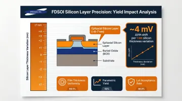
Epitaxial layer quality and thin-film electrical properties are tied directly to device performance: switching speed, power consumption, and operating reliability. In FDSOI devices, threshold voltage changes by approximately 4 mV per 1 nm of silicon thickness variation, meaning precise epitaxial layer control is essential for parametric yield.
Off-spec film properties discovered late in processing result in entire wafer lots being scrapped or downgraded—tight process control using hydrogen at the deposition stage prevents this.
KPIs impacted:
- Film thickness uniformity
- Layer electrical resistivity
- Parametric yield
- Lot acceptance rate
When this matters most:
This advantage is especially critical for logic chip manufacturers (where transistor layer precision defines performance class), memory fabs (where film uniformity across billions of cells determines retention and reliability), and LED manufacturers (where epitaxial layer composition controls emission wavelength and efficiency).
Advantage 3: Equipment and Process Protection Across Advanced Manufacturing Steps
Hydrogen provides protection at multiple points in the fab:
In EUV lithography systems: Hydrogen reacts with tin debris deposited inside the light collector to form volatile stannane (SnH₄), which is removed by vacuum. Without this, tin buildup degrades EUV optics and drives expensive unplanned maintenance. High-NA EUV scanners represent over $300 million in capital investment, and unplanned downtime can cost more than €1 million per 24 hours.
In ion implantation: Hydrogen blocks tungsten transport in the ion source by capturing free fluorine radicals to form HFₓ, preventing formation of volatile WF₆. This extends tool stability and component lifetime.
In chemical storage: Hydrogen stabilizes reactive mixtures such as diborane (B₂H₆) and digermane (Ge₂H₆), which decompose without it, reducing shelf life and increasing waste.
Why equipment protection affects total cost of ownership:
EUV tools carry some of the highest capital costs per unit in a fab, and unplanned downtime on these systems has an outsized cost impact. Degraded reactive gases also introduce hidden impurities and quality drift that may not surface until wafer-level testing—by which point the cost of failure is fully sunk.
KPIs impacted:
- Tool uptime
- Mean time between maintenance
- EUV optic service interval
- Reactive gas shelf life
- Chemical spend per wafer out
When this matters most:
This matters most at fabs running EUV lithography for sub-7nm nodes, in facilities with high volumes of ion implantation steps, and at any operation that stores and uses reactive hydrogen-containing process chemicals.
What Happens When Hydrogen Quality or Supply Falls Short
Sub-specification hydrogen purity and inconsistent supply don't always surface immediately. Contamination from persistent impurities — including CH₄, N₂, or moisture — can cause gradual yield degradation, off-spec film properties, or crystal defects that only appear during final device testing.
Oxygen impurity spikes (such as 1E20 atoms/cm³) in SiGe films contribute to mobile charges and interface trap charges, degrading device performance. Even at parts-per-million levels, impurities in hydrogen affect wafer yield and process stability.
Supply inconsistency compounds these quality risks. When hydrogen delivery falters during critical process steps, the downstream consequences extend well beyond a single missed operation.
How Supply Gaps Disrupt Fab Operations
- Reactive gas blends that are not properly stabilized decompose in storage, requiring emergency replenishment and creating scheduling gaps
- Hydrogen supply shortfalls during EUV or annealing operations halt those process steps entirely, disrupting downstream steps and creating fab-wide schedule risk
Why Failures Rarely Stay Isolated
Hydrogen quality or supply failures generate cascading costs beyond the immediate disruption:
- Scrapped wafers
- Unplanned tool maintenance
- Emergency gas procurement at premium prices
- Engineering time spent diagnosing process excursions that trace back to gas quality rather than equipment or process recipe issues
How to Get the Most Value from Hydrogen in Electronics Manufacturing
Hydrogen delivers its full operational advantages only when purity is consistently maintained at specification. For semiconductor applications, this typically means ultra-high-purity grades (99.999% and above). SEMI C58 provides specifications for semiconductor-grade hydrogen, with 6.0 Grade (99.9999%) hydrogen specifying limits of ≤0.5 ppm for H₂O, O₂, and N₂, and ≤0.1 ppm for hydrocarbons.
Any source of impurity introduction—cylinder condition, transport handling, or degraded reactive gas blends—can quietly erode yields and process consistency. Working with a specialty gas supplier that provides verifiable purity standards and NIST-traceable documentation is the practical safeguard against that variability.
Maintaining Blend Stability in Reactive Process Gases
For facilities using hydrogen-stabilized reactive process gases like diborane or digermane mixtures, the stability of those blends over time is as critical as the initial purity. Proprietary cylinder treatment and blending techniques—such as SpecGas's internal cylinder treatment process, developed through decades of reactive gas R&D— prevent in-storage decomposition that would otherwise introduce impurities or require frequent reordering.
Building Gas Purity Into Process Audits
Review process outcomes regularly against established KPIs. If defect density climbs, film properties drift, or tool maintenance intervals shorten without a process recipe change, hydrogen quality or supply consistency should be among the first variables examined. Building gas purity verification into routine process audits keeps this input from becoming a hidden source of yield variability.

Conclusion
Hydrogen's value in electronics manufacturing comes from three converging capabilities: uniform heat transfer for defect-free annealing, chemical precision that governs layer growth and deposition quality, and protective effects that extend tool life while preserving reactive chemical integrity. Each of these directly shapes yield, uptime, and cost at the process level.
These advantages compound only when hydrogen purity and supply are treated as controlled process inputs rather than commodities. Inconsistent gas quality introduces variability that traces back to the source — which is why verifiable purity standards and reliable supply matter as much as the gas itself.
Frequently Asked Questions
How is hydrogen used in electronics?
Hydrogen serves four main applications in electronics manufacturing: annealing (uniform heat transfer to repair crystal damage), epitaxy (reducing agent for layer growth), thin-film deposition (controlling electrical properties), and chemical stabilization (extending reactive gas shelf life). Newer uses include EUV lithography chamber cleaning and ion implantation source protection.
What purity level does hydrogen need to be for semiconductor manufacturing?
Semiconductor-grade hydrogen requires a minimum purity of 99.999% (5.0 Grade) or higher, with 99.9999% (6.0 Grade) common at advanced nodes. Even trace impurities at parts-per-million levels can affect process yield and film quality. Purity requirements become stricter as device node sizes shrink below 7nm.
What role does hydrogen play in EUV lithography?
EUV light is generated by firing a laser at tin droplets, which deposits tin debris inside the tool's light collector. Hydrogen reacts with this debris to form volatile stannane (SnH₄) that is removed by vacuum pump, keeping optics clean and extending maintenance intervals on tools that cost over $300 million each.
How does hydrogen affect yield in semiconductor fabrication?
Hydrogen's uniform heat transfer reduces crystal defects during annealing, and its precise reducing-agent chemistry during epitaxial layer growth keeps film properties on spec. Both mechanisms directly reduce the rate of wafers that fail parametric or end-of-line testing, improving cost-per-good-die.
What are the safety considerations for using hydrogen in electronics manufacturing?
Hydrogen is highly flammable, burns with a nearly invisible colorless flame, and forms explosive mixtures with air across a wide concentration range (4.0% to 75.0% by volume). Fabs operate under NFPA 2, NFPA 55, OSHA 29 CFR 1910.103, and SEMI S2 protocols, with mandatory leak detection and controlled storage and handling systems.
Is on-site hydrogen generation better than packaged supply for electronics fabs?
Both approaches are used. Packaged supply (cylinders or tube trailers) suits lower-volume or flexible needs, while on-site generation (via electrolysis or steam methane reforming) may suit high-volume fabs consuming hundreds of Nm³ per hour.